OptiStack® multilayer lithography systems are designed for the most advanced high-volume semiconductor manufacturing processes in the world. Our versatile OptiStack® material set is designed to be used in combination with our proprietary optical modeling to achieve the finest resolutions possible with 193-nm immersion lithography.
The OptiStack® system advantage
A universal substrate – OptiStack® materials work together to planarize a wide range of topography, effectively creating a "universal substrate" for advanced processes.
Superior optical performance – OptiStack® modeling systems work with unique paramaters to yield superior pattern fidelity to that of standard modeling systems.
High aspect ratio capabilities – OptiStack® materials maintain excellent pattern fidelity even at extreme aspect ratios.
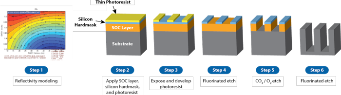
How OptiStack® multilayer systems work
OptiStack® multilayer systems use a combination of a thick, carbon-rich underlayer, a thin silicon hardmask, and a thin photoresist to achieve accurate pattern transfer to the substrate. Some scenarios also require an additional bottom anti-reflective coating (BARC) beneath the photoresist.
After the thin photoresist is imaged, the pattern is transferred to the silicon hard mask (Si-HM, also known as a spin-on glass or SOG) using a highly selective etching process, such as fluorinated plasma. The pattern is then transferred to the carbon-rich underlayer (known as a spin-on carbon or SOC) with another selective etching process, typically an oxygen-rich plasma. The imaged hardmask and SOC layers can then be used to transfer the pattern to the substrate.
Why we need multilayer lithography systems
Immersion lithography requires the photoresist to be extremely thin due to the shallow depth of focus inherent in high-NA optical systems. At these thicknesses, the photoresist can no longer survive the etching steps required to transfer the pattern into the substrate. The additional materials in a multilayer stack essentially work to magnify the etch resistance of the photoresist.