Brewer Science is revolutionizing packaging with innovative thin wafer handling (TWH) technologies. Our diverse set of high-performance materials allow for higher throughput, reduction in form factor, and lower cost. We work with leading equipment vendors to provide fully automated solutions for high-volume needs.
Talk to an Expert Today
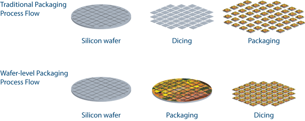
Wafer-level packaging (WLP) is the technology of packaging the die while it is still on the wafer—protective layers and electrical connections are added to the substrate before dicing. Originally, wafers were diced into individual chips, then packaged. Utilizing WLP technology allows chips to continue to reduce in size, streamlines manufacturing, and provides easier ways to test chip functionality.
To create new stacked designs, manufacturers must find ways to thin their device wafers before performing complex back-end processes. Using temporary bonding techniques, in which the wafer is attached to a stable carrier without disrupting back-end processes, can overcome this problem.
Moore’s Law originally stated that the number of transistors would double every two years. However, the timeline has changed to 18 months. Moore’s Law has proven useful in the semiconductor industry as a way for companies to guide long-term planning and set targets in research and development.
Since physical limitations to transistor scaling are being reached, moving beyond Moore’s Law has become a necessity. More-than-Moore Technology (MtM) focuses on creating new technological possibilities with unlimited application potential through research and development past already conventional methods.
Brewer Science has been using its materials expertise in the semiconductor industry to change the way the world looks at advanced packaging for over 15 years. With collaboration from our research, development, and applications groups we have become one of one of the largest advanced packaging knowledge centers in the world; creating the largest portfolio of products in the industry.
Packaging Solutions