Permanent Bonding Materials

PermaSOL® Materials
Request More Information on Permanent Bonding Materials

PermaSOL® Materials

PermaSOL® materials address a range of needs identified for permanent bonding applications, which include low-temperature bonding, excellent chemical resistance, thermally curable bonding process and no material movement after the bonding process.

Talk to An Expert Today

Permanent Bonding - Circuits

Advantages of Permanent Materials:

  • Adhesive for permanent applications
  • Target thickness range 1-20 µm
  • Low dielectric constant
  • High chemical resistance
  • High adhesion to various substrates
  • Room-temperature bonding
  • No squeeze-out or material movement after cure
  • Thermally cured system

Key Marketing Drivers Enhanced by Permanent Bonding:

  • MEMS devices including glass frit and anodic bonding technologies in order to achieve good hermeticity to protect the MEMS sensor
  • LED devices requiring metal bonding (eutectic and thermo-compression bonding) to meet higher performance in terms of light extraction
  • CMOS image sensors for direct bonding & adhesive bonding
  • SOI substrate manufacturing supporting the fusion bonding technology
  • 3D integration utilizing thermo-compression bonding (TCB)

Process Flow

What are Permanent Bonding Materials?

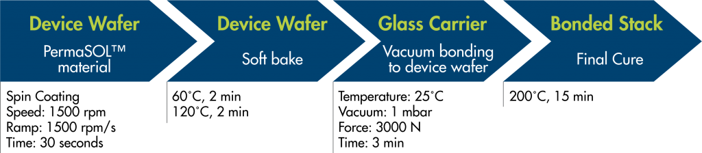
Permanent bonding materials are adhesives used to assemble IC logic chips, memory chips, image sensor devices, and microelectromechanical systems (MEMS) devices that go into high-density heterogeneously integrated packages. These high-density, ultra-thin electronic packages are needed for artificial intelligence (AI) in high-performance computers, data centers, 5G, and high-end mobile products.

Contact Us

Contact Us

Permanent Bonding Materials

Top