Making a Difference in the World Through Our People & Technology
Explore 40 Years of InnovationZero Defects Mindset
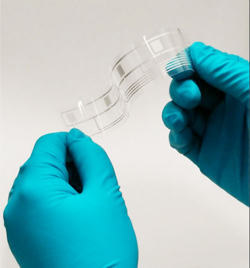
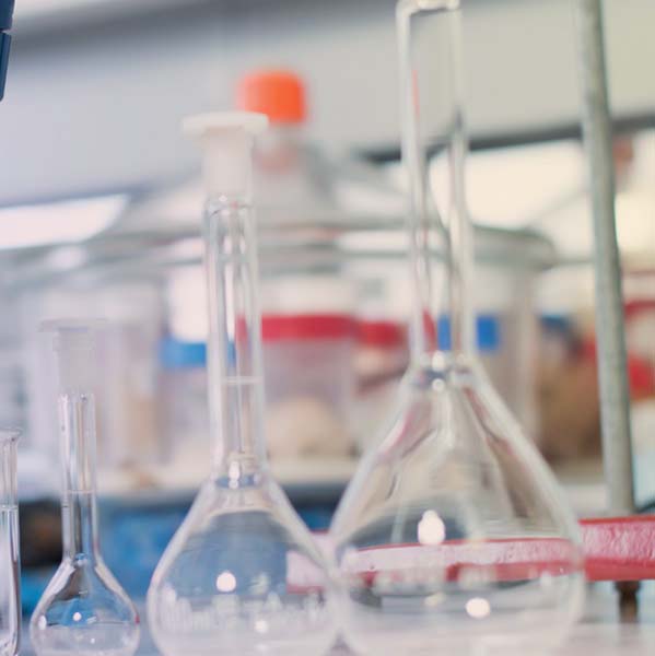
Materials Right the First Time
At Brewer Science we focus on technology innovation as a pathway forward by providing the highest quality products to our customers through our focus on zero defects and manufacturing perfection.
Our Commitment to Zero Defects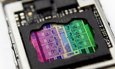

Solutions for Equipping the Technologists of Tomorrow
Within our organization, we believe that freedom, combined with clear objectives and commitment to growth, will bring about the biggest innovations.
Read More About Our Company
World Class Support
Every member of our team is focused on helping our customers reach their technology goals through our results-oriented approach to problem solving.
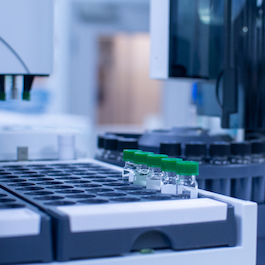
Expert Research Capabilities
Brewer Science has been a technology leader in the fields of specialty materials and equipment for micro- and optoelectronics since 1981. By creating innovative products and technologies, Brewer Science maintains a competitive edge in new and future markets.
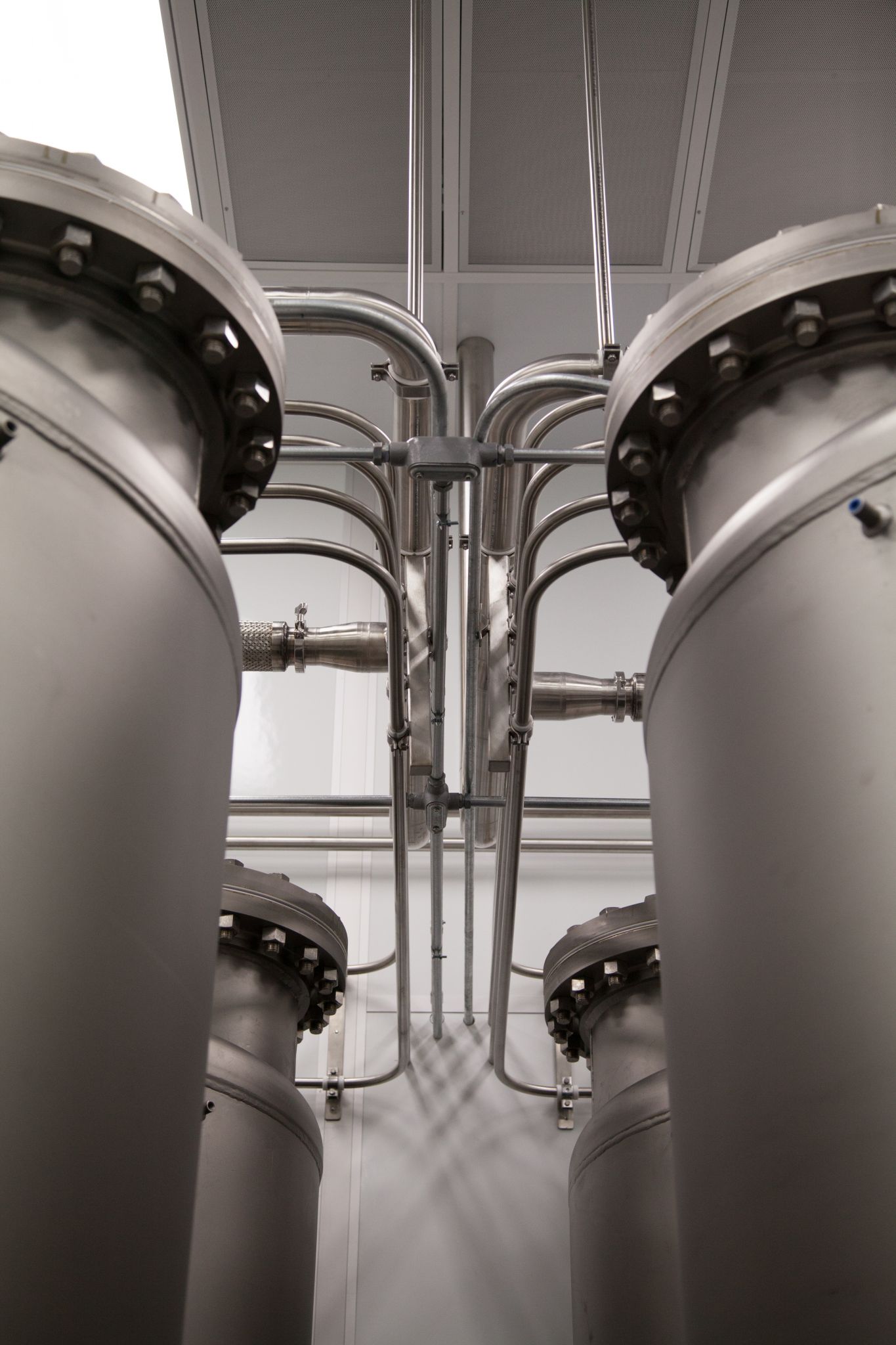
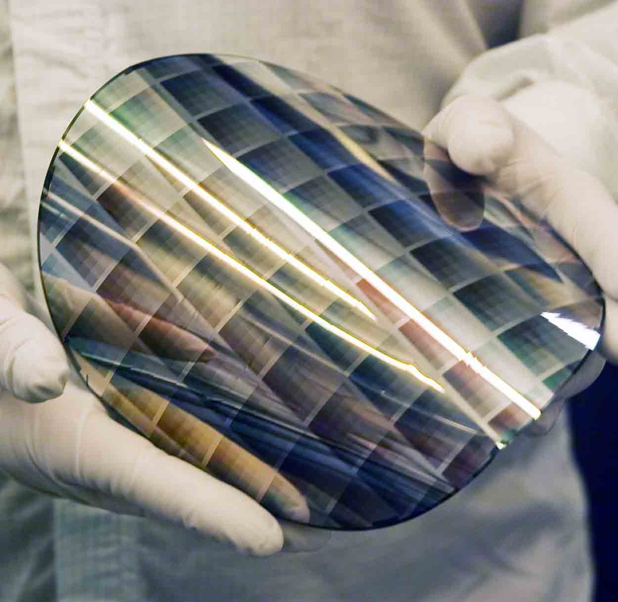
Manufacturing Excellence
There are reasons top companies engaged in the semiconductor and electronics industries rely on Brewer Science products for their advanced nodes; our promise is to ensure that products supplied by Brewer Science are the most reliable and consistent in the industry.
Sustainability in the Workplace
Brewer Science is focused on creating quality products and processes that are not harmful to the environment and do not deplete natural resources, and support long-term ecological balance for generations to come.
Click to Learn More
99.7%
of hazardous waste was mitigated through fuel blending or metal recovery in 2022.

233.5 Tons
of solvent wastes were diverted from landfill in 2022.

124%
of energy consumption offset from wind energy in 2022 (at Rolla and Vichy location)

52 Tons
of waste materials recycled in 2022
 Going Green at Brewer Science
 "Of the People" - 40 Years of Innovation
 Our Anthem