Products
Experience the difference with Brewer Science's revolutionizing technologies. We offer an extensive range of products, from lithography materials to equipment, that impact our everyday lives.


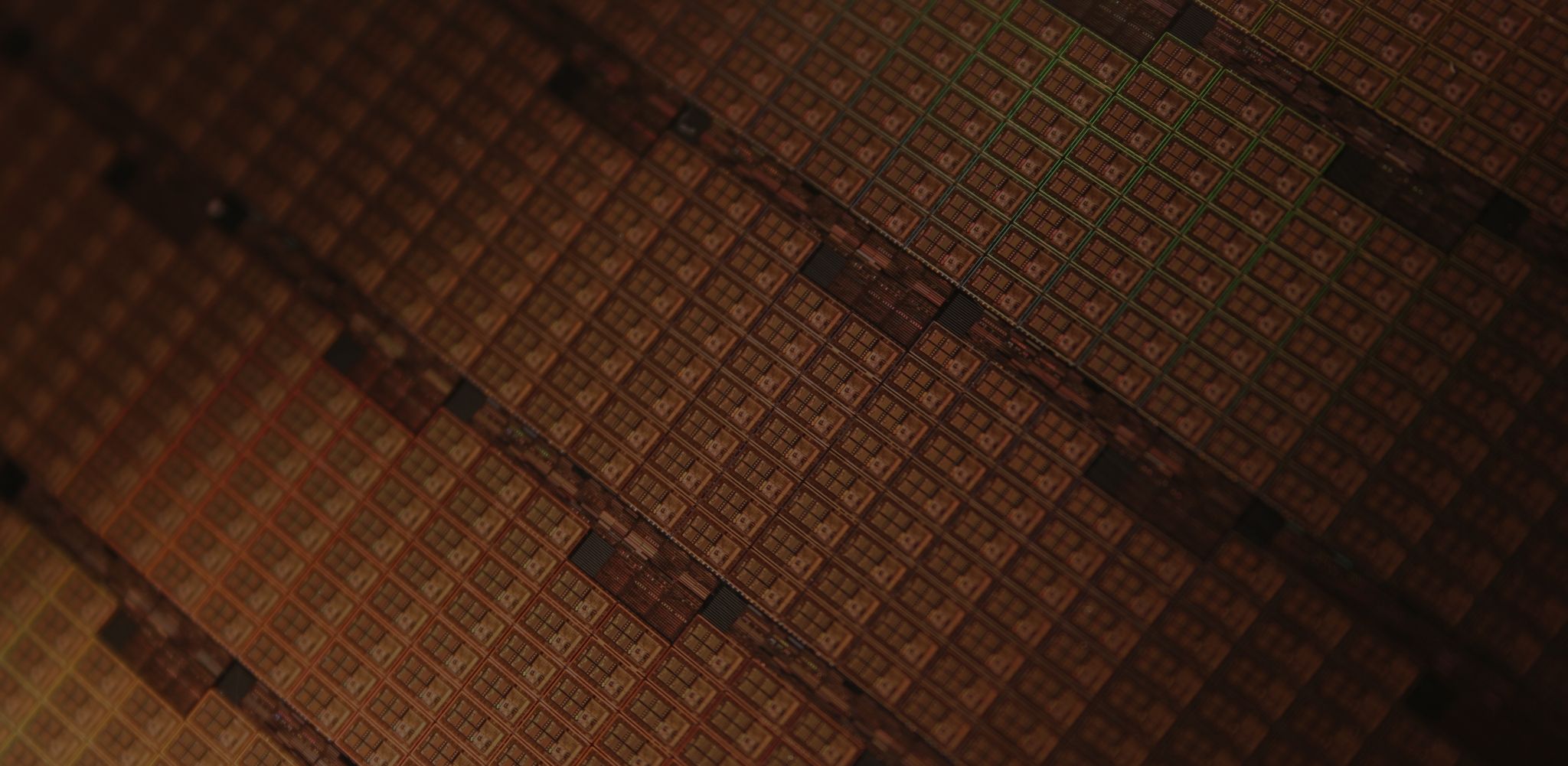
Brewer Science lithography products have been shaping the semiconductor industry since 1981. Over the years, new product lines, capabilities, and specifications have been improved to deliver the best


BrewerBOND® T1100/C1300 Series Materials enable our unique VersaLayerTM system for high-temperature and high-stress applications found within the semiconductor industry.
Brewer Science is proud to offer an extensive program dedicated to exploring new realms of sensor performance – environmental monitoring.
Brewer Science’s integrated sensor system is an automated system that enables more predictive analytics.
The biggest problem facing lithographers using EUV is the RLS trade-off: simultaneous improvement of resolution, line width roughness, and photosensitivity.
Brewer Science is changing how environmental and process data is captured, transmitted, and analyzed using custom-designed printed electronics systems.
BrewerBOND® 530 mechanical debonding release material offers additional choices for stronger adhesions necessary for high stress/high temperature temporary bonding applications.
OptiStack® multilayer systems are our flagship lithography technology, and are used for leading-edge high volume IC manufacturing.
ProTEK® B3 coatings thin films are spin-applied polymeric coating systems that provide temporary wet-etch protection for CMOS MEMS circuitry during alkaline or acid etches.
ARC® antireflective coatings are the industry benchmark for reflection control and light absorption during photolithography.
Temporary wafer bonding release material for mechanical debonding applications
This UV laser release material was designed to benefit a variety of temporary bonding, debonding market applications including chip-first/chip-last and RDL-first FOWLP processes.
BrewerBOND® 305 temporary wafer bonding material is an organic coating that enables back-end-of-line (BEOL) processing of ultrathin wafers using standard semiconductor equipment.