September 2 – 4, 2026
Taipei, Taiwan
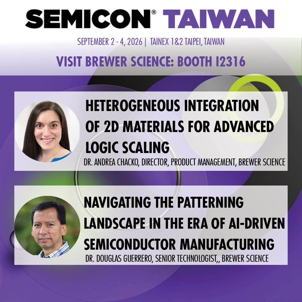
Please visit Brewer Science at Booth I2316.
Brewer Science will be exhibiting and presenting at SEMICON Taiwan 2026.
SEMICON Taiwan
September 2 – 4, 2026
Taipei, Taiwan
Please visit Brewer Science at Booth I2316.
Presentations
Navigating the Patterning Landscape in the Era of AI-Driven Semiconductor Manufacturing
Presented by Dr. Douglas Guerrero, Senior Technologist at Brewer Science
Abstract
Artificial intelligence is driving the most rapid technology adoption in history, fundamentally reshaping the global digital economy. As the industry races to meet the demands of AI and high-performance computing, chip manufacturing is pushing the limits of both logic and memory architectures. Behind these advancements, materials suppliers are engineering the largest, most complex set of patterning materials ever seen.
While the number of semiconductor manufacturers implemented the latest patterning technologies has consolidated over the years, the ecosystem of specialized materials suppliers has increased. This presentation will share how Brewer Science leverages its advanced materials portfolio to navigate this shifting landscape, ensure supply chain resilience and deliver the high-selectivity, patterning and advanced packaging solutions critical for next-generation lithography.
Heterogeneous Integration of 2D Materials for Advanced Logic Scaling
Presented by Dr. Andrea Chacko, Product Manager at Brewer Science
Abstract
The continued scaling of silicon-based CMOS is increasingly constrained by fundamental electrostatic limits, motivating the exploration of alternative channel materials and device architectures. Two-dimensional (2D) semiconductors, particularly transition metal dichalcogenides (TMDs), offer a compelling pathway to extend logic scaling beyond these limits.
The handling, transfer, and integration of ultrathin, mechanically fragile layers present significant manufacturing challenges. A key challenge lies in the sequential integration of multiple 2D layers without compromising the integrity of previously fabricated device tiers. Direct high-temperature growth techniques such as chemical vapor deposition (CVD), while suitable for high-quality 2D material synthesis, can degrade underlying layers.
To address this limitation, heterogeneous integration through low-temperature transfer methods has been explored. In this approach, individual 2D layers are first synthesized independently on optimized donor substrates at elevated temperatures (>800 °C) to ensure high crystalline quality. These layers are then transferred and stacked onto target wafers at reduced temperatures, preserving the structural and electronic properties of both the transferred material and the underlying device layers.
This work highlights how established semiconductor packaging solutions—specifically temporary bonding and debonding (TBDB) materials traditionally used for wafer support during back grinding—can be repurposed to address these challenges. Leveraging proven TBDB platforms, this study explores their application in the transfer of 2D materials, enabling precise handling and integration into device structures.