Nine Essential Criteria to Achieve a Successful Bonding Process
A photosensitive permanent bonding material enables the creation of high-quality permanent bonds between dissimilar materials used in the creation of MEMS and sensors. Having a thorough understanding of the materials and product performance is crucial to the success of the end application. In this article, we explore nine criteria used to evaluate a polymeric photosensitive permanent bonding material. These criteria include Process Flow, Chemical Resistance, Photolithography, Transparency, Film Uniformity, Defectivity, Thermal Stability, Bonding, and Shear Strength.
Process Flow
Processing on wafer enables the fabrication of complex structures and patterns on a large scale, which offers significant advantages in terms of cost and time-to-market. To ensure efficient and effective processing on wafer, consider using materials that demonstrate:
- High Resolution
- Chemical Resistance
- Thermal Stability
- Low Moisture Absorption
- Low Exposure Dose
- Low Cure Temperature
- Short Cure Time
This graphic illustrates an example of an in-house process flow for photosensitive permanent bonding materials using a standard thermal compression bond.
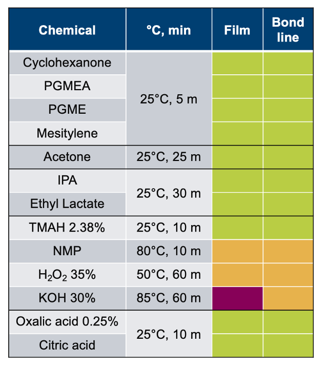
Chemical Resistance
The permanent bonding material should be resistant to downstream chemicals used in the application, as well as survive environmental factors that may affect the bond quality over time. When testing the photosensitive permanent bonding material, a wide range of chemical exposures are done to the exposed film and to bonded pairs to ensure versatile applications.
This table provides performance examples of the chemical resistance tests used to evaluate our photosensitive permanent bonding materials.
Photolithography
For photosensitive permanent bonding applications, the use of photolithography allows for precise control over the placement of the bonding material, ensuring that it is present only where it is needed. This helps to minimize excess bonding material and reduce the risk of damage to the substrate. Additionally, photolithography can be used to create specific shapes or patterns in the bonding material, which will improve the performance of the bonded device.
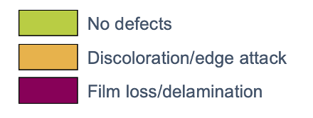
Beyond 40-µm pitches, hybrid bonding becomes an attractive alternative to microbumps. A typical hybrid bonding process targets critical dimension (CD) sizes below 10 µm. The fine pitch patterning capability of the photosensitive permanent bonding material supports its use for dense die-to-die interconnection.
Below are actual images of an exposure matrix performed using silicon substrates with an exposure dose < 200 mJ/cm2 L/S, achieving CD sizes of 6 µm and 3 µm.
Transparency
Film transparency is a concern for devices such as optical sensors, where transmission of light through the bonded device is crucial to the success of the application. However, for photovoltaic devices, some absorption of light by the bonding material may be desirable. Light transparency of a photosensitive permanent bonding material is a measure of the film’s ability to allow light at given wavelengths to pass through it. The visible light spectrum is the section of electromagnetic radiation that is visible to the human eye usually defined as wavelengths between 400-700 nm.
This graph illustrates the transparency when processed on a quartz wafer, using the best known methods to create the test sample, there is greater than 95% transmittance between 405 – 800 nm.
![]()
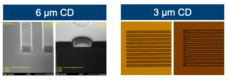
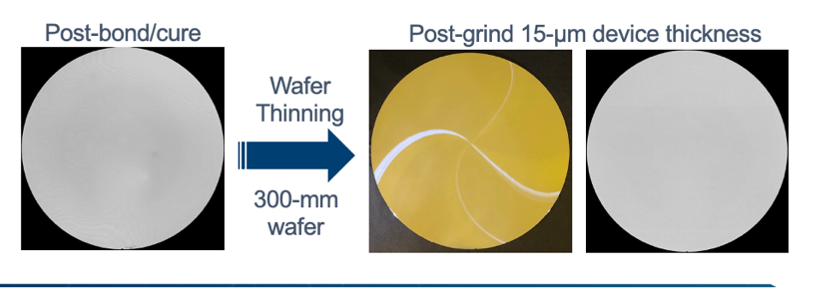
Film Uniformity Film total thickness variation (TTV) is important in applications that use photosensitive materials since variations cause distortion in the transmitted image or signal in optical devices. For MEMS, TTV can affect the mechanical properties of the device, leading to issues such as stiction and reduced reliability.
To ensure optimal performance and reliability of the bonded device, it is important to minimize TTV in the bonding material. This can be achieved through careful control of the deposition process, substrate preparation, and bonding conditions. For example, the use of polishing or planarization techniques can help to reduce substrate surface irregularities that contribute to TTV. Additionally, the use of bonding processes that allow for controlled compression or deformation of the bonding material can help to reduce variations in thickness. Process improvements such as auto dispense, controlled air flow in coater and edge bead removal are all options that may minimize film edge effects and improve film TTV.
Copper-polymer and polymer-polymer hybrid bonding require zero defects with coplanar bonding surfaces with minimal surface roughness. This improves bond formation, yield and reliability which are critical to achieving interconnect functionality.
This is an image of the bond line by scanning acoustic microscopy (CSAM) done on flat wafers without topography and no planarization.
Defectivity
Defectivity is an important factor to consider when selecting bonding materials for photosensitive applications as defects significantly impact the quality and performance of the final product. If the bonding layer has high defectivity, it can lead to:
- reduced device yield
- decreased performance
- device failure
Defects in the bonding material can cause voids, cracks, and delamination, which can result in electrical, mechanical, or optical failures. These defects can also lead to changes in the material properties, such as reduced adhesion strength, increased stress, and altered thermal properties, which can affect the long-term reliability and stability of the device.
Therefore, it is crucial to select bonding materials with low defectivity and high reliability for photosensitive applications to ensure optimal performance and durability of the final product. Various factors can affect the defectivity of bonding layers, such as purity of the materials, processing conditions, and the bonding techniques used. Careful consideration and testing of the bonding materials are necessary to minimize defects and ensure the quality and performance of the final product. Brewer Science takes a rigorous approach to material selection, working with suppliers to ensure materials meet a part-per-quadrillion level of purity.
Making to Zero Defects – Brewer Science
Thermal Stability
Thermal stability by thermal gravimetric analysis (TGA) is required for evaluating the decomposition behavior of the bonding material. In photosensitive applications, the thermal stability and decomposition behavior of the bonding material can have a significant impact on device performance and reliability. For example, in high-temperature applications such as power electronics, the bonding material may be exposed to temperatures that can cause thermal degradation or decomposition. By characterizing the thermal stability and decomposition behavior of the bonding material using TGA, it is possible to ensure that the material can withstand the operating conditions of the device without compromising its performance or reliability.
TGA can also be used to optimize the processing conditions of the bonding material by identifying the temperature range and conditions under which the material decomposes or volatilizes. This information can be used to optimize the deposition and curing process to ensure that the bonding material is fully cured and stable while minimizing the risk of decomposition or volatilization.
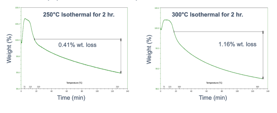
Good thermal stability of the permanent bonding material is a necessary requirement for the successful implementation of a hybrid bonding process. To strengthen the bond and form electric contact at the interconnects, a thermal anneal process of bonded pairs is performed at temperatures >250°C under a vacuum. TGA was also conducted to determine the decomposition temperature for fully cured films. At 350°C in N2, a 2% weight loss was measured. At 400°C a weight loss of 5% was observed.
This line chart illustrates the thermal stability, noting the weight loss deviation within a two-hour timeframe a 250°C and 300°C isothermal conditions in N2.
Bonding When selecting a permanent bonding material for a photosensitive application, it is important to consider the properties of the materials being bonded, the processing conditions, and the operating environment. The bond must be able to withstand mechanical, thermal, and environmental stresses that the device may encounter during its lifetime. Failure of the bond can lead to catastrophic failure of the device, rendering it useless.
We test these scenarios in different applications including chip-to-chip (C2C) and chip-to-wafer (C2W) using SiO2 to the permanent bonding material. We also evaluate polymer-to-polymer bonding.
There were no voids or defects observed post-annealing at 200°C for one hour. These CSAM images were generated to evaluate the bond quality.
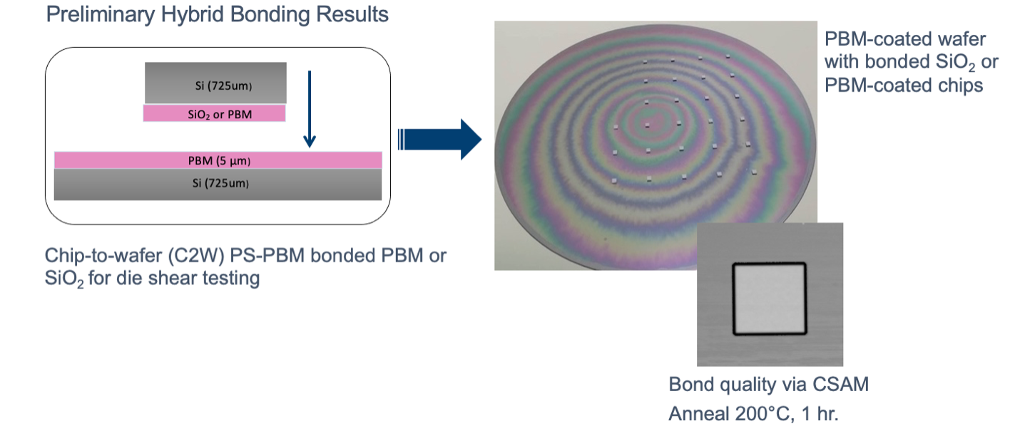
Image illustrates an example of a chip-to-wafer process using photosensitive permanent bonding material (PS-PBM)
Shear Strength
Selecting a permanent bonding material with high shear strength is essential for ensuring the reliability and longevity of applications and can help to avoid potential failures and costly repairs or replacements in the future. In optoelectronics, shear strength is important for bonding structures such as lenses, prisms, and filters to other components of the device, where the bond must withstand the weight of the component and transmittance.
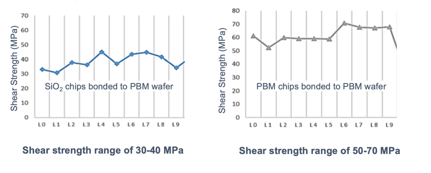
Using an xyztec bond tester, the peak load (force) was measured and represents the maximum amount of shear force the bond line can handle before failure. Using a blade, increasing force is applied to the side of the chip until the blade induces to induce a failure by fracture. The amount of force required to cause this failure is known as shear strength. These tests indicate a shear strength range of 30-40 MPa for SiO2 bonded to PBM and a range of 50-70 MPa for PBM chips bonded to PBM wafers.
To understand the performance of a material, an evaluation of nine criteria is necessary. Process Flow, Chemical Resistance, Photolithography, Transparency, Film Uniformity, Defectivity, Thermal Stability, Bonding, and Shear Strength are important properties for successful performance. Overall, a photosensitive permanent bonding material is an important tool for creating high-quality, permanent bonds between different materials for use in the microelectronics industry. By better understanding the material’s performance characteristics and product properties, you can assess which material is best suited for your application. Learn more about Brewer Science’s permanent bonding materials on our website.