An Overview of Temporary Wafer Bonding Processes

Consumer electronics such as smartphones, tablets, and handheld devices are driving the demand for thinner, smaller, and more highly integrated semiconductor packages. Wafer-level packaging (WLP) is evolving rapidly to shrink package sizes for easier incorporation into mobile electronic devices. Semiconductor die or ‘chip’ sizes have continued to decrease, creating the need for new package designs that provide greater bandwidth and higher pin counts to interconnect the chips. Historically, the packaging industry has relied on flip-chip processing for most WLP applications. Over the last few years many new forms of WLP have been developed to enable higher-density applications, namely fan-out WLP (FOWLP), fan-in wafer-level chip-scale packaging (FI-WLCSP), 3 D FOWLP, 2.5-D integration with interposer technology, and true 3-D IC integration using through-silicon via interconnects. Many of these WLP technologies involve processing of thin wafers that must be mechanically supported during the manufacturing flow. Temporary bonding is proving to be a reliable method for handling and processing thin device wafers. In this method, a device wafer is temporarily adhered to a rigid carrier wafer with a polymeric material. The properties of the polymeric bonding material largely control the stability of the entire structure during thinning and other processing.

The Temporary Bonding Process

The temporary bonding process consists of reversibly mounting a device wafer to a carrier wafer with a polymeric bonding material system. The bonding materials and the carrier wafer mechanically support the device wafer during thinning (back-grinding) and subsequent backside processing that includes processes such as deposition, dry and wet etching, plating, and cleaning, among others. Since the primary bonding material and its ancillary layers control the bonding and debonding characteristics as well as the in-process stability of the structure, they must be carefully designed to withstand the high stresses created by thermal cycling, coefficient of thermal expansion (CTE) mismatch, layer deposition, and a host of other factors while remaining easily separable at the end of the process.

Contact Bonding

Two main temporary bonding processes, contact bonding and thermo-compression bonding, have evolved that utilize very different polymeric bonding materials. Contact bonding uses a liquid-like curable adhesive layer that is coated onto a transparent carrier wafer. The carrier is typically ultra-smooth glass that has a thin light-to-heat conversion layer on the surface that is in contact with the adhesive layer. The device wafer is placed in contact with the coated carrier and a small amount of pressure is applied to cause the adhesive material to flow in and around the features on the device wafer surface. The structure is held in this position while the adhesive layer is cured in place by exposing it to UV light through the transparent carrier. Curing converts the adhesive layer into a 3-D polymer network that is resistant to flow even at elevated temperatures.

Debonding or separation of the structure after backside processing has been completed involves exposing the light-to-heat conversion layer through the carrier with a near infrared laser, which decomposes the layer and in turn releases the carrier for removal. The cured adhesive layer is then peeled as a sheet from the device wafer by an automated instrument. A drawback of contact bonding is that the peeling process often leaves adhesive residues that are very difficult to remove on the surface of the device wafer. Moreover, the peeling force can be sufficient to damage or dislodge metal features on the device wafer surface.

Thermo-Compression Bonding

Thermo-compression bonding utilizes a thermoplastic bonding material rather than a curable adhesive material. Thermoplastic polymers do not crosslink or cure when heated but instead reversibly soften and then re-harden to a glassy state when cooled to room temperature. For temporary bonding purposes, thermoplastic bonding materials are usually designed to soften and flow sufficiently at about 200°C so that they will fill in and around device features and bond to the device wafer under pressure (typically 5-10 psi). At room temperature, they form a stiff, resilient bond line that allows processes such as wafer grinding to be performed without deformation occurring. However, it is also important that the bonding materials retain sufficient cohesive strength and resistance to flow for the bonded structure to remain mechanically stable during backside processes that can reach temperatures as high as 250°C or more. The ability of a thermoplastic bonding material to meet these requirements can be best determined by examining its melt viscosity across the expected temperature use range.

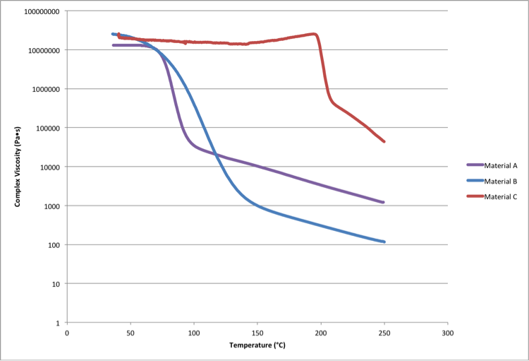
The figure below (please note the logarithmic scale on the vertical axis) displays the complex (melt) viscosity versus temperature profiles for three thermoplastic bonding material platforms over the range of 50°-250°C. The sharp drop in melt viscosity exhibited by Material A near 75°C corresponds to the glass transition temperature (Tg) of the material. At the Tg, the material transitions from a glassy state to a rubbery state, and then as temperature further increases, to a (very) viscous liquid state. Material B undergoes a more gradual but much larger decrease in melt viscosity within the same temperature range as Material A. Material C has an exceptionally high Tg and does not soften appreciably to well beyond 250°C, and as such it would not be useful in typical temporary bonding processes. While Materials A and B are viscous liquids at 200°C, it should be noted that the melt viscosity of Material A is more than ten times greater than that of Material B at this point, which means it can tolerate much more stress without delaminating, voiding, or deforming than Material B. Based on melt viscosity characteristics and other parameters such as adhesion strength and wetting, thermoplastic material platforms can be chosen and optimized for temporary bonding applications that require different bonding temperatures and that present different levels of stress during backside processing.

table

Debonding of Temporarily Bonded Structures

There are three principal modes of debonding used with thermoplastic bonding materials.

  • Slide Debonding. This mode of separation takes advantage of the reversible softening behavior of thermoplastic bonding materials. In this mode, the bonded structure is heated above the softening temperature of the bonding material and an opposing shear force is applied to the device and carrier wafers, causing them to slowly slide past one another until the structure is separated.
  • Laser Debonding. In this mode, a transparent carrier wafer is coated with a thin (ca. 1 µm) laser-sensitive polymer layer that ablates, that is, decomposes into gaseous byproducts and a small amount of carbonaceous residue, when irradiated through the carrier with a scanning laser. The thermoplastic bonding material adheres to the laser-sensitive layer on the carrier side of the structure. In some cases, the bonding material itself will ablate when exposed to the laser radiation and a separate laser-sensitive layer is not required in the bond line. Laser debonding is performed with a variety of laser types. Early systems operated at near-infrared wavelengths (> 1000 nm). The next generation of laser debonding equipment moved to using shorter wavelength radiation (530 nm). The most recently introduced systems have employed pulsed excimer lasers that emit in the ultraviolet range (248 nm, 355 nm) to achieve higher scanning speeds (i.e. higher wafer throughput) and to reduce the amount of post-ablation residue.
  • Mechanical Debonding, which is sometimes called peel separation. In this case, peeling does not refer to removing a polymeric layer from the device wafer. Rather, it refers to separating the structure at an interface between the bonding material and a surface-treated carrier wafer or a second polymeric layer coated onto the carrier wafer. The bonding material and the surface treatment or second polymer layer are designed to have sufficient adhesion at their interface that the bonded structure can survive normal in-process stresses but not be so strongly bonded that a high force, which could break the thin device wafer, is needed to separate between the layers. The debonding process involves initiating a crack between the two layers at the edge of the structure and then propagating the crack across the entire interface between the layers using very low force to cause separation. The use of a thermoplastic bonding material and a low-surface-energy polymeric release layer, which can be a curable or thermoplastic composition, are preferred for most mechanical debonding situations.

General Thermo-Compression Bonding and Debonding Process Flow

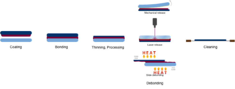
The general process flow for thermo-compression bonding and subsequent debonding of a thin device wafer is illustrated in the figure below.

processflow

The more detailed elements of the steps in the flow can be explained as follows:

  • Edge Trimming – It is now a common practice to trim or recess the edge of the device wafer back by about 0.5-1.0 mm with a specialized grinding tool. The grinding process creates a square edge on the device wafer so that when it is thinned it is not so susceptible to cracking and chipping at the edge. Edge trimming can be performed prior to or after temporary bonding.
  • Coating – A thermoplastic bonding material is spin-coated onto the device wafer and baked in 2-3 stages to remove solvents. The outer edge bead of the coating is sometimes removed with solvent to prevent it from squeezing out into the bevel area of the wafer edge where it can catch contaminants and crust over during backside processing, eventually making debonding more difficult. The laser or mechanical release layer is coated onto the carrier wafer and baked. In some instances, the bonding material is applied directly over the release layer rather than applying it separately onto the device wafer. Co-application of the two layers can reduce post-bond total thickness variation (TTV) of the bonded structure, especially when the device wafer surface has a high density of tall metal features such as copper pillars or C4-style solder bumps.
  • Bonding – Thermo-compression bonding is performed in an evacuated chamber to ensure that gas-filled voids are not trapped in the bond line or around surface features by the bonding process. The coated device and carrier wafers are aligned and brought into contact between platens that are heated to the bonding temperature. A compressive force is applied through the top platen to cause the thermoplastic bonding material to spread and flatten so that the device and carrier wafers are as co-planar as possible (measured back-to-front). The bonded structure is removed from the bonding chamber and slowly cooled to room temperature to prevent stress accumulation in the bonding material.
  • Thinning and Backside Processing – A host of processes can be applied to the bonded structure after thinning. The important thing is that the bonding material system does not allow the bonded structure to distort or delaminate under the stresses imposed by these processes. It should be noted that temporary bonding is being used increasingly for applications where the device substrate is not thinned but is difficult to handle during backside processing because of its propensity to warp or bow severely in response to temperature changes and stresses created by deposited layers. Embedded die (reconstituted) wafers are a good present-day example of a difficult handling challenge.
  • Film Frame Mounting – A thinned device wafer should never be in a freestanding condition. Therefore, it is customary to bond the device wafer to a film frame prior to debonding the carrier wafer. This allows the device wafer to be handled safely after the supporting carrier has been removed from the structure.
  • Debonding (carrier removal) – The prevailing methods of debonding were presented above. In the temporary bonding processes where Brewer Science materials are employed, debonding always refers to removal of the carrier by one of these three methods.

Cleaning – The debonding process leaves the thermoplastic bonding material on the device wafer. An important advantage of using thermoplastic bonding materials is that, unlike curable bonding materials, they can be removed with solvents and organic cleaners after processing to leave a residue-free device wafer surface. Moreover, wet cleaning with solvents imposes no mechanical stress on the fragile device wafer. Modern automated tools are able to clean the device wafer while it is attached to a solvent-compatible film frame. A second part of the cleaning process pertains to the carrier wafer. In many cases, the carrier wafer can be reutilized after stripping in a piranha solution or an organic solvent, followed by aqueous cleaning, to remove bonding material residues and particulates from various deposition and etching processes.

Brewer Science Temporary Bonding Materials

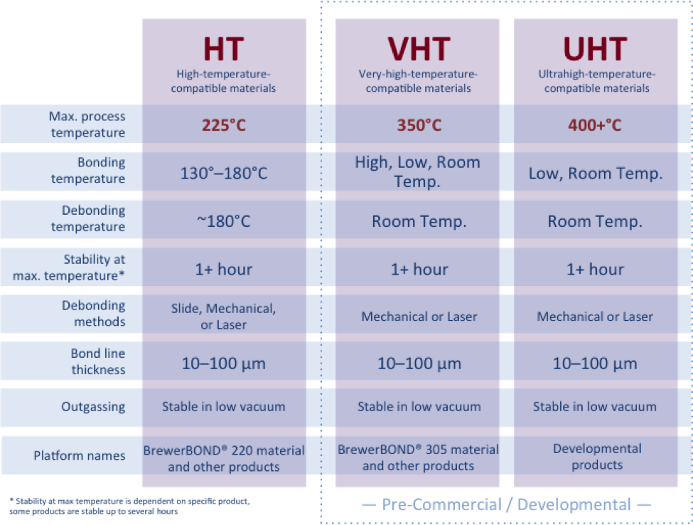
Brewer Science has a broad portfolio of thermoplastic bonding materials and companion mechanical and laser release layers designed for different use conditions and substrate types. The information in the table below is a high-level classification of the temporary bonding materials that are available and being developed by Brewer Science for different applications. Several of these platforms are already used in high-volume production while others are pre-commercial materials that are currently undergoing field testing and customer evaluations in advanced applications.

In our experience, three main-use temperature ranges exist: high temperature (HT, 175°-225°C), very high temperature (VHT, 225°-350°C), and ultrahigh temperature (UHT, 350°-400°C+). Within these classifications, one can select specific products for compatibility with different bonding and debonding methods, tool designs, and other process flow requirements. Our VHT and UHT material platforms have been developed mainly for room temperature debonding by laser or mechanical release.

Material_table

The industry is moving toward higher-temperature processing of thinner, more highly stressed, larger-area wafers and panels. All the while, the expectations for temporary bonding materials are moving toward more simplified bonding and debonding processes at lower temperatures and with less force to improve yields and throughput and reduce process cost-of-ownership. Consequently, we expect to see dynamic changes in the roadmap for temporary bonding materials and process development over the next few years.